SiC Epi Doping
A highly precise technology
The Energy-Filter technology guarantees high precision epi layer doping and improved thickness uniformity. Chip manufacturers are guaranteed higher device yield and quality alongside substantially improved cost efficiency.
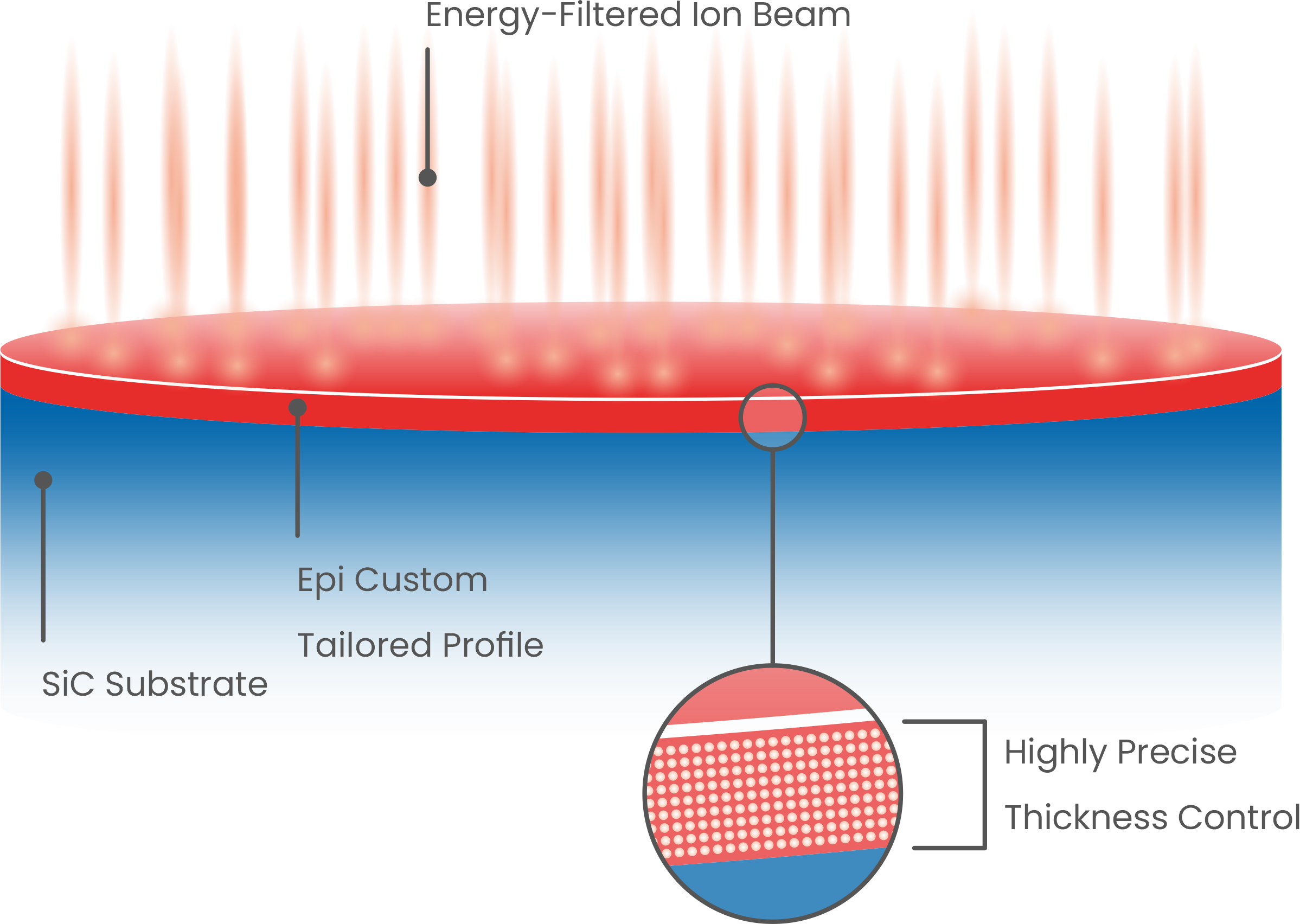
SiC Diode Drift Zone
Doping with highly augmented accuracy
Our cutting-edge Energy-Filter technology provides exceptional n-type drift zone doping for 600V-1200V SiC power devices.
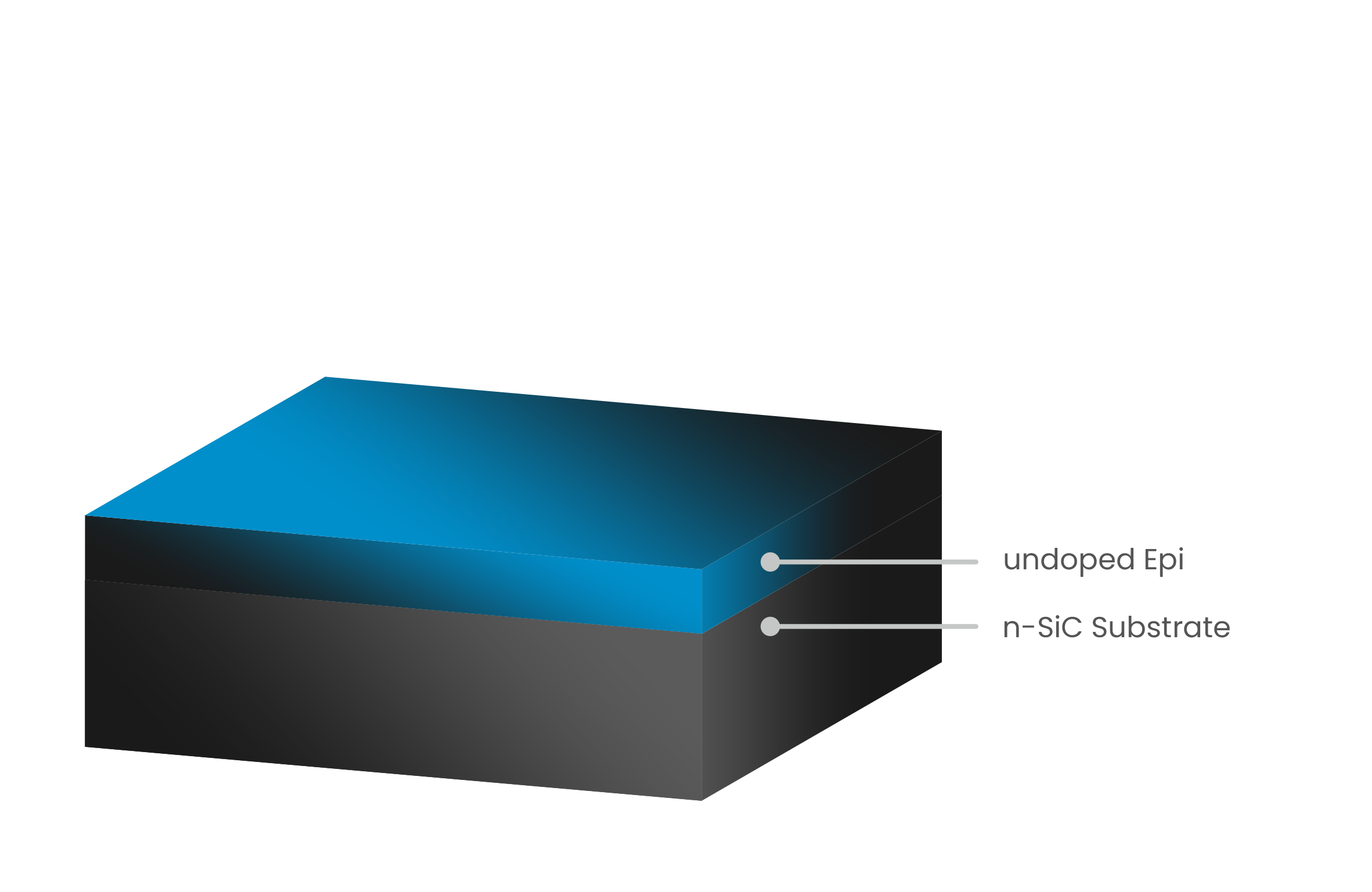
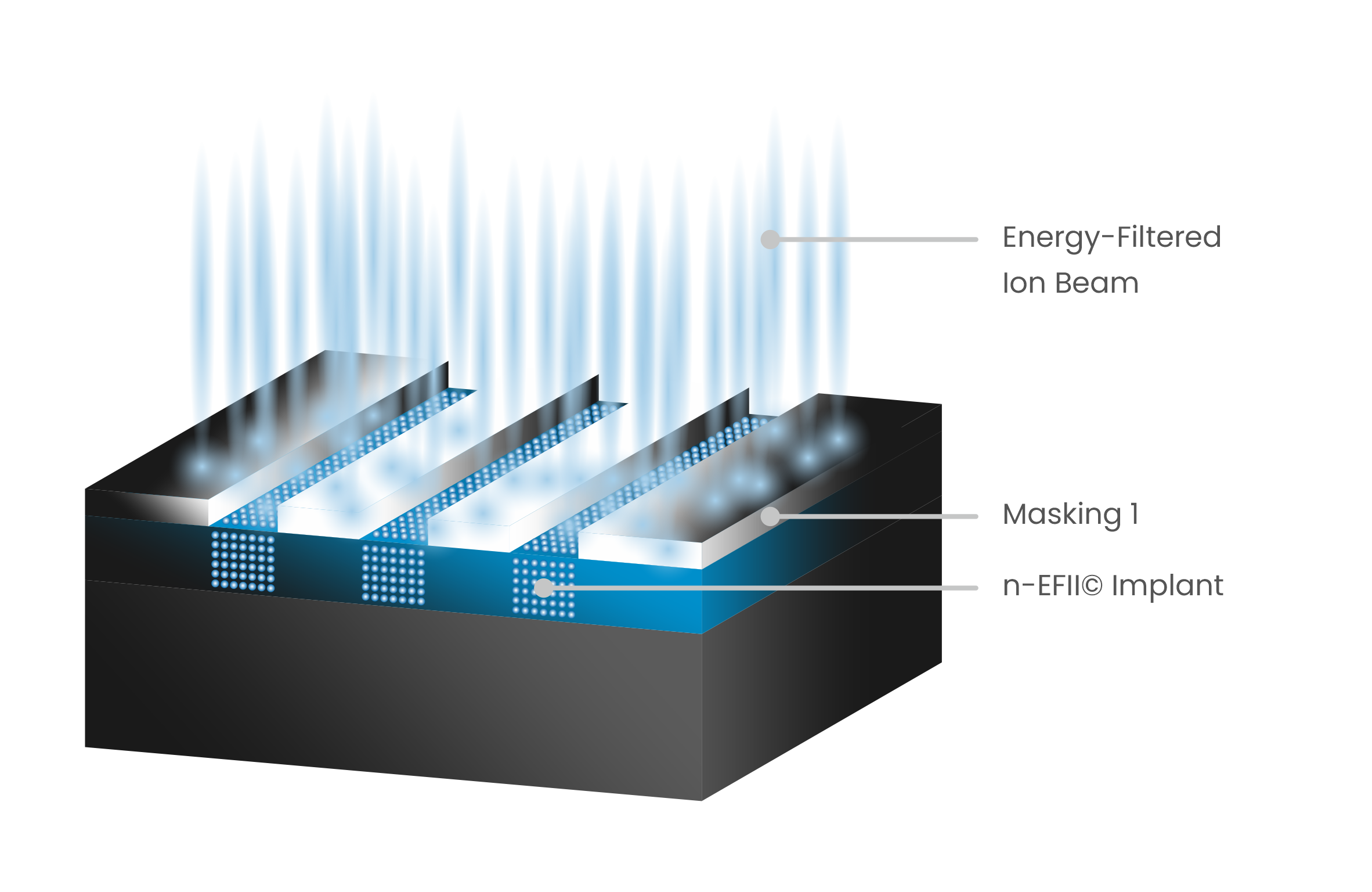
We recommend using undoped epitaxial layer formation followed by the Energy-Filter process to manufacture n-type drift zones. This method will help to realize previoulsy unattained levels of doping uniformity.
Benefits
mi2-factory’s blanket Nitrogen-EFII© process results in drift-zone doping with highly augmented accuracy:
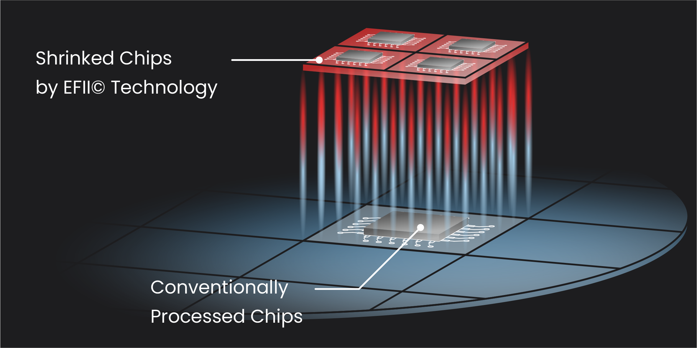
direct cost benefit for MPS diodes and MOSFETs
potential chip shrink of over 30% for 1200V MPS diodes
tighter distributions of forward voltage drop and breakdown voltage
Applications
more than
30%
chip shrink potential
less than
3%
depth range variation
less than
3%
doping inhomogeneity
Results from packaged chip data
Our test vehicle – the 650V SiC MPS diode from Infineon Technologies – has provided robust and compelling proof of the Energy-Filter technology’s succesful translation to and suitability for commercial settings and applications. The IQR/median value of packaged diodes is much smaller for chips processed with EFII© technology than for conventional chips. Forward characteristics up to 10x 12A*.


*data from joint project between Infineon Technologies AG and mi2-factory GmbH, 2015
Alternative highly homogenous drift layer doping for 650V SiC devices (R. Rupp et al, Materials Science Forum, ISSN: 1662-9760 Vol. 858, pp 531-534)
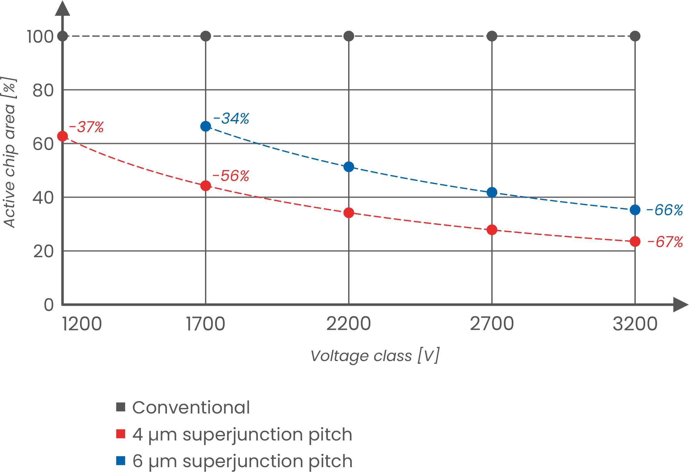
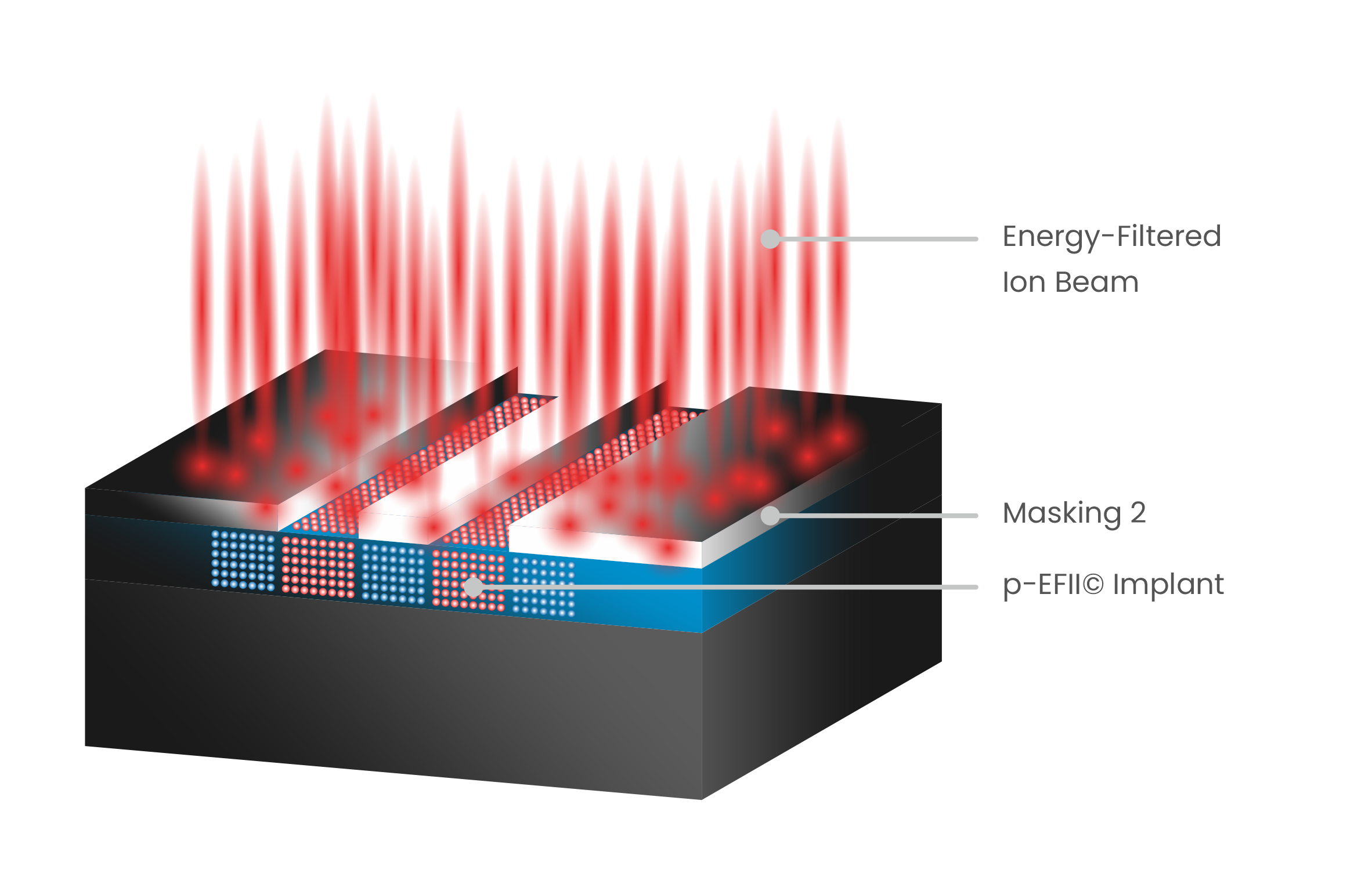
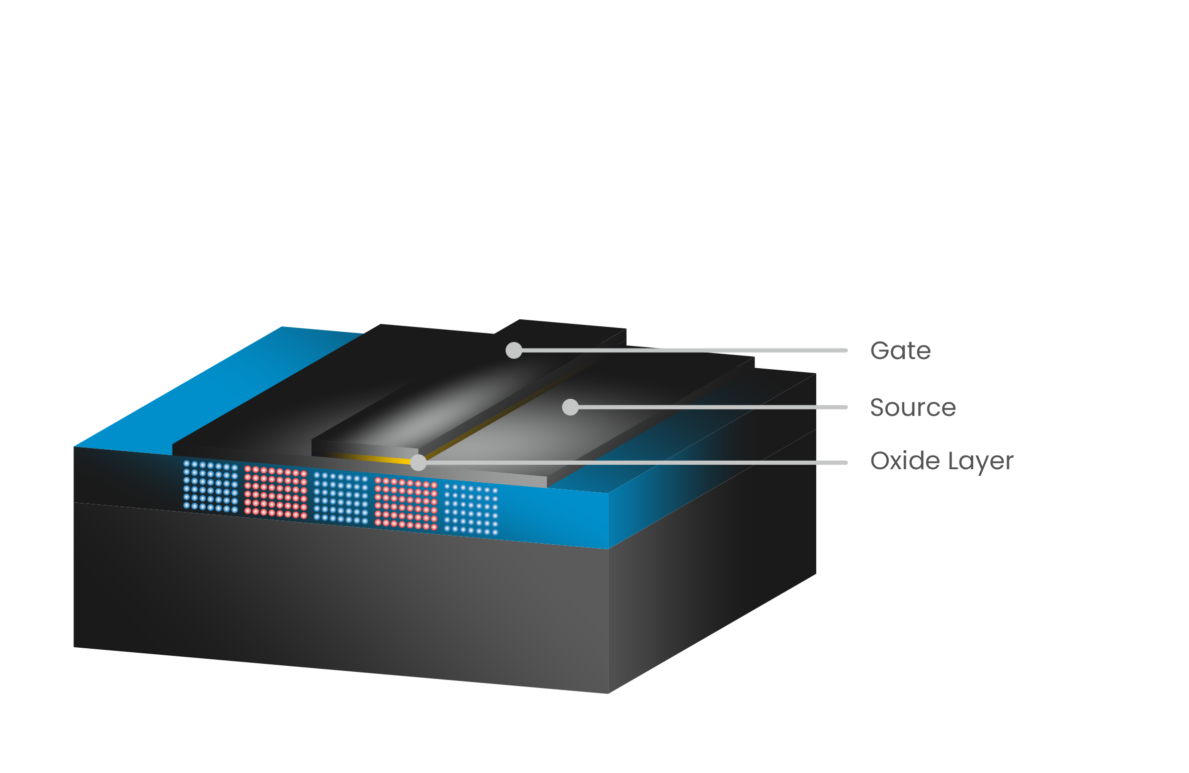
SiC Superjunction MOSFET
A powerful technology for your powerful MOSFETs
1.2kV SiC superjunction (SJ) MOSFETs are superior in cost-performance compared to conventional MOSFETs. But how to manufacture a SJ structure in SiC? Our approach: multiepitaxy with masked EFII© p- and n-implant.
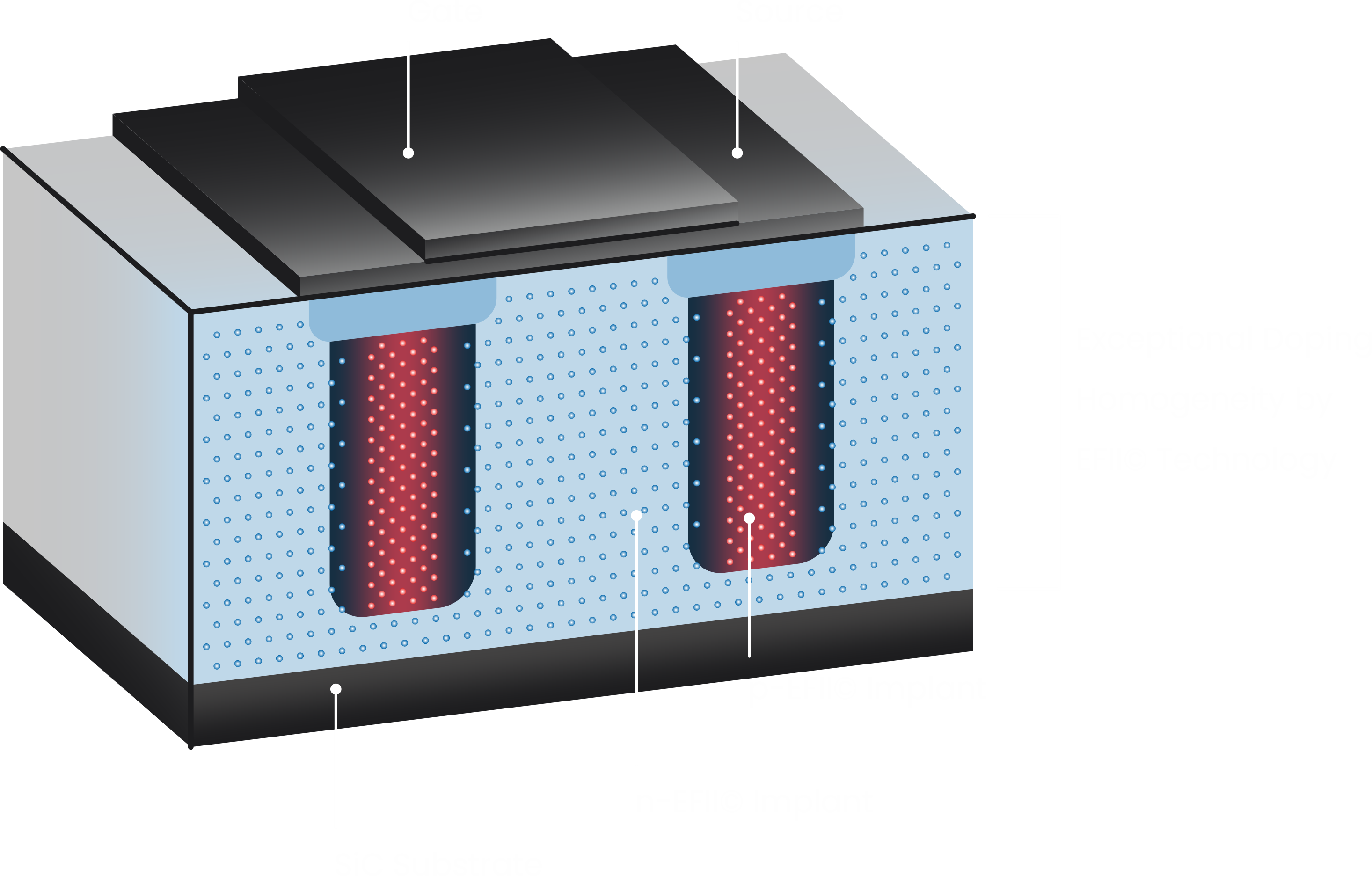
Approach
Our approach of multiepitaxy with masked EFII© p- and n-implants enables cost-effective manufacturing of superjunction structures in silicon carbide. Our technology provides specialized implantation and undoped epi regrowth.
Applications
Active chip area reduction
In the graph below, the active chip area reduction afforded by SiC Superjunction MOSFETs relative to conventional SiC MOSFETs is visualized.